www.pnlabvn.com


 Ảnh sản phẩm thuộc về PNLAB
Thông tin chi tiết sản phẩm |
|||
Tên sản phẩm: |
ALTERA FPGA EP4CE6F17C8 |
||
Giá: |
2.400.000 |
||
Tình trạng: |
Liên hệ |
||
Xuất xứ: |
China |
||
Hãng sản xuất: |
Pnlab |
||
Mã sản phẩm: |
EP4CE6F17C8DV |
||
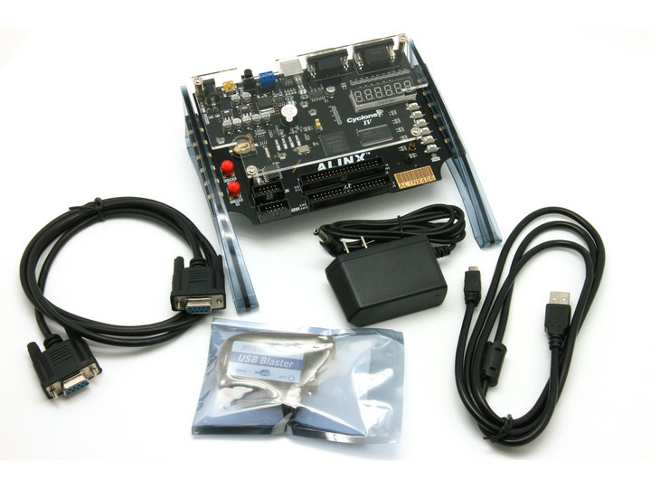
Packing list :
1. FPGA development board 1 set
2 serial line 1
3. 5V/2A Power 1
4 matching CD 3
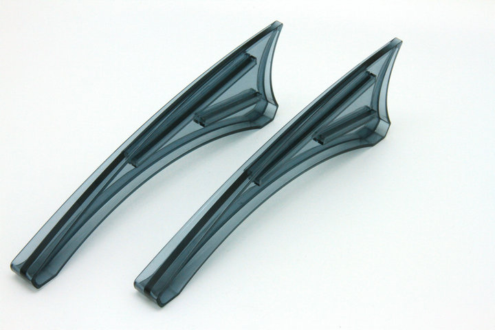
5 The circuit board holder 2
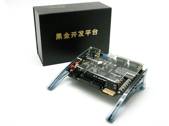
6 beautifully packaged box 1
7. USB downloader 1 (need to shoot suit connected, or not provided)
The new Series 2013 student edition listed the upgraded version! ! ! ! !
The 2013 Student Edition for a new design. We customize a unique insulated bracket, making the development of insulated panels and other objects to ensure the stable operation of the development board.
PE insulated bracket using materials with good insulation, and very beautiful, unique design, the entire development board is also extremely beautiful.
Supporting information
In fact, everyone is looking to buy development board information, so we talk about our supporting information below
Our biggest feature is the black gold has a wealth of original data, and the data is continually updated
Take a look at four verilog tutorial tutorial it
Literacy and three other full content of this verilog tutorial directory Download (Copy the following address into your browser's address bar):
http:pan.baidu.com/share/link?shareid=3936048202&uk=2131212159
We have tested, 11.0sp1 version of the software has a very good stability under Win7 system, developed by NIOS II compatibility issues do not appear, but the compilation speed has been greatly improved .
NIOS and original supporting Verilog tutorial:
"NIOS II that thing" rev7.0 ( the most classic and most influential NIOS II Tutorial by our engineers AVIC eds );
"Verilog HDL gift - Verilog HDL Literacy text" ( for the classic Verilog syntax summary, very helpful for beginners );
"Verilog HDL those things - modeling chapter" rev4.0 ( constructed the first chapter of the primary modeling, detailed explanation of the primary modeling method );
"Verilog HDL those things - Timing articles" rev2.0 ( content is to create a sequel to upgrade knowledge in modeling on the basis of articles );
"Verilog HDL kept private private drizzle - Integration Concepts" ( integration concept is based on articles and timing modeling papers, written communication module built );
"Verilog HDL kept private private drizzle - and the length of the clock signal" ( This article is about the clock along the relevant content, the content is more in-depth );
"Verilog HDL try to stop the rain - ideal timing of integration" ( written about the IIC and SDRAM driven content to a higher level of depth );
"Messing around TimeQuest no obligation notes - first" ( for a detailed explanation TimeQuest first );
"Messing around TimeQuest no obligation notes - The second" ( for a detailed explanation TimeQuest The second );;
"FPGA development board user guide black gold" ( black gold for FPGA development board general introduction, and the first step in guiding the development board );
Above the original tutorial pages have reached around 1500, integrated into a 400-page book has been close to 4. 4 books supporting a development board can say is unprecedented.And above content is far from over, we will continue to write original tutorial in 2012. Please always pay attention to our black gold, Dongli District, http://www.heijin.org (copy and paste into the address bar).
Supporting video tutorials:
"NIOS II that thing" video tutorial (Original) (updated to 16 sets);
ALTERA FPGA official video tutorials (43 sets);
Zhou, who Verilog video tutorial (5 episodes chapter 7);
Xia Wen Verilog video tutorials (16 episodes) ;
Development Board Structure
Planar structure of the entire development board is shown below (two pictures below correspond to each other):
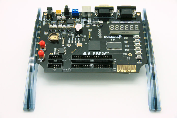
Throughout the development board detailed resources :
Through this diagram we can see that we can achieve this development platform functionality.
We use a 5V power supply and USB-powered two ways, please remember that the power supply can not be in two ways at the same time, at the same time, can only supply one way, or it may burn the computer's USB port .
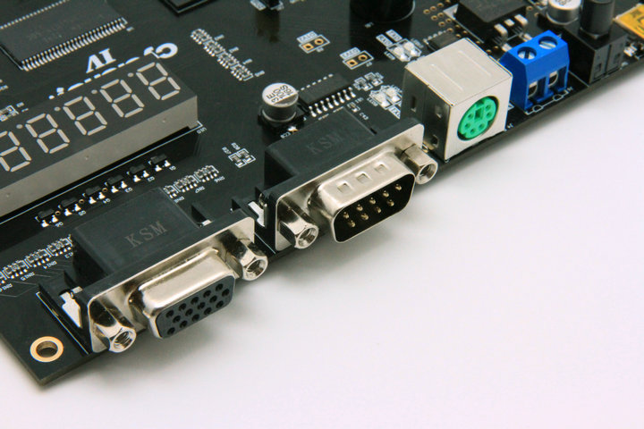
· way RS485 interface, standard 485, can not communicate with other devices;
· other devices do not communicate the way RS232 interface, the standard 232 interface with computers;
· the way PS / 2 interface, you can access PS / 2 mouse or keyboard interface;
· one VGA port, VGA port to 16bit, you can display 65,536 colors, you can display color photographs and other information.
· one of the RTC real time clock with battery holder, battery model CR1220.
· an IIC EEPROM interface 24LC04;
· a buzzer, enabling SOS alarm function;
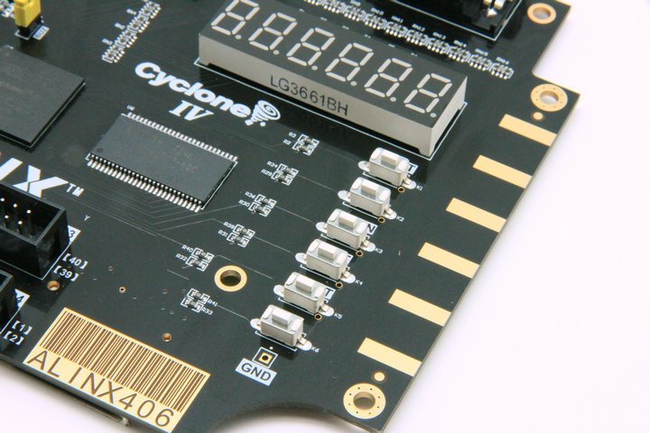
· 6 were positive digital control, dynamic scanning, dynamic display numbers;
· a 256Mbit SDRAM, which can be used to cache data can also be used as memory NIOS running;
· 4 light-emitting diode LED;
· 6 independent keys;
· Onboard 50M active crystal, the development board to provide a stable clock source;
· one external clock input interface SMA;
· one clock output interfaces SMA;
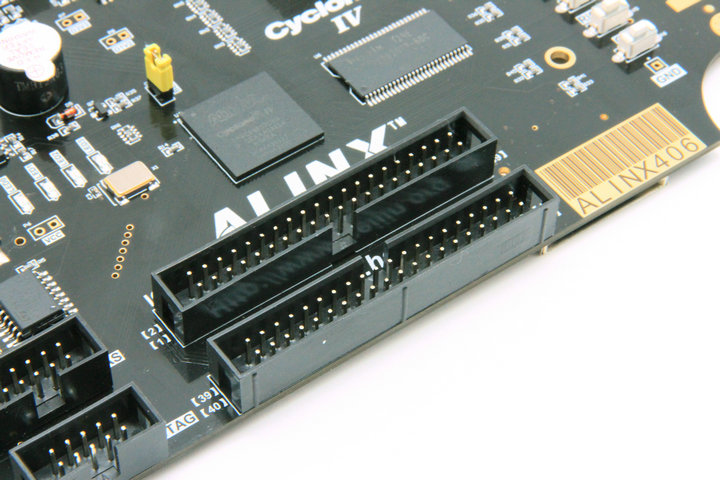
· 2-way 40-pin expansion port (2.54mm pitch), of which 34 IO ports, 1 5V power supply, 2 3.3V power supply, 3-way GND. Total extension of 68 3.3V IO port, you can also pick TFT modules and AD / DA module expansion module.
· AS reserved JTAG port and port, debug and program the FPGA cured.
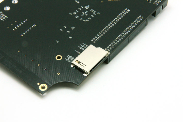
· 1 SD card connector, SD card support SPI mode and 4bit bus mode.
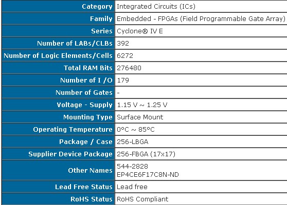
FPGA chip models: EP4CE15F17C8
The 2013 Student Edition is CYCLONE IV series FPGA, model: data EP4CE6F17C8N, ALTERA official as follows:
Wherein the main parameters
Logic unit LE: 6272; prefix = "o"
Multiplier LAB: 392;
RAM : 276480bit;
IO number: 179;
Core voltage: 1.15V-1.25V (recommended 1.2V);
Operating temperature :0-85 ℃
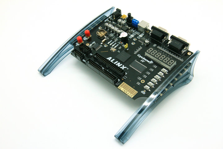
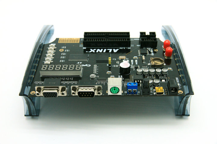
Development board overall picture
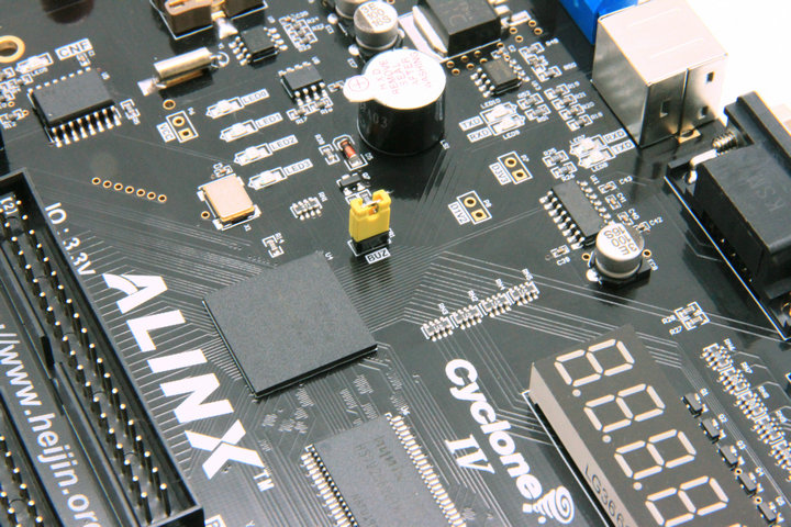
FPGA development board partial picture: Power section
Extensive use of electrolytic capacitors, while four-layer PCB design, with separate power and GND, to ensure a stable power development board
Three-way power supply: 3.3V, 2.5V, 1.2V;
Power Interface: USB interface and power supply interface (while only using one, do not simultaneously access)
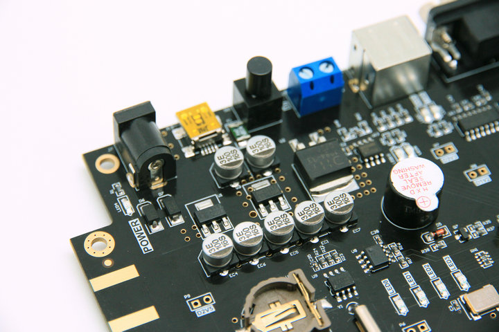
FPGA development board partial picture: Power section
Set aside a total of 68 separate IO statement users (no sharing with other chips).
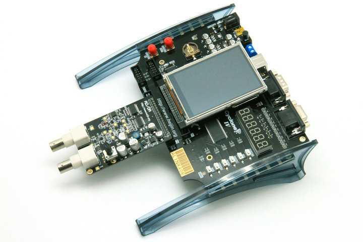
Two expansion port, which can take two black gold expansion modules, such as ADDA, TFT32
Below is simultaneously connected to two modules.
FPGA development board partial picture: SDRAM, keys, digital
FPGA development board partial picture: VGA interface, RS232 serial port, PS2 interfaces, RS485 interface (from left to right)
FPGA development board partial picture: SD card, back in the development board